

The electronics industry demands high precision stamping parts that operate at dimensional tolerances an order of magnitude tighter than general industrial stamping—often ±0.001 inches and finer on critical features—while maintaining surface finishes and edge quality that enable reliable electrical contact, precise connector mating, and secure solder joints. This is not the stamping world of structural brackets and chassis panels. High precision stamping parts for the electronics industry are miniature, tight-tolerance, and functionally critical—where a dimensional error of 0.0005 inches can mean the difference between a reliable connector and a field failure. This article explains the technical requirements, manufacturing methods, and supplier qualification criteria that define high precision stamping parts for electronics industry applications.
Precision Tolerance Requirements for Electronics Stamping Parts
High precision stamping parts for electronics applications operate in three tolerance bands that define their manufacturing method and cost structure. Standard precision stamping—achievable on conventional stamping equipment—holds ±0.005 to ±0.010 inches on features above 0.050 inches in size. High precision stamping parts—requiring precision-ground die components, servo-feed control, and in-process inspection—hold ±0.001 to ±0.005 inches. Ultra-precision high precision stamping parts—requiring specialized micro-stamping equipment, carbide tooling, and environmental temperature control—hold tolerances below ±0.001 inches, achievable only by stamping service providers with dedicated micro-stamping capabilities.
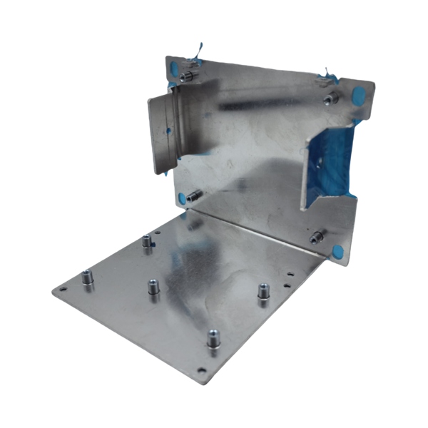
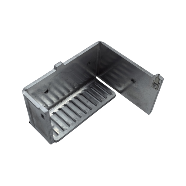
Connector Stamping Parts: Tolerance and Spring Design Requirements
Electrical connector high precision stamping parts—pin contacts, socket contacts, grounding springs, and tab contacts—are the most demanding precision stamping category in the electronics industry. Connector spring contacts must maintain a defined normal force within a specified deflection range to ensure reliable electrical continuity through the mating interface. This spring function imposes both dimensional tolerances on the stamped geometry (deflection range) and spring rate requirements (force-deflection relationship) that are sensitive to the stamped material's yield strength, work hardening rate, and residual stress state. The stamping die design for connector high precision stamping parts must account for springback compensation, stress relaxation during storage and assembly, and the effect of plating thickness on the final spring geometry. Material selection for connector high precision stamping parts is driven by the required spring force, conductivity requirements, and environmental exposure—beryllium copper alloys (C17200, C17510) for high-conductivity spring applications, phosphor bronze (C51900) for moderate conductivity and good spring properties, and stainless steels for environments requiring both spring function and corrosion resistance.
Terminal and Pin Stamping Parts: Fine Blanking Versus Conventional Stamping
Electronic terminal high precision stamping parts with square, hexagonal, or non-round cross-sections require fine blanking (precision blanking) rather than conventional stamping to achieve the required edge squareness, dimensional accuracy, and surface finish. Fine blanking uses a V-ring impression in the die face that applies hydrostatic compressive stress to the material immediately surrounding the cut perimeter, suppressing the brittle fracture and rollover that produces the rough, angled cut edges characteristic of conventional stamping. Fine blanked high precision stamping parts achieve cut edge squareness of 89 to 90 degrees (versus 82 to 87 degrees for conventional stamped parts), surface finishes of Ra 16 to Ra 32 µin as-blanked, and dimensional tolerances of ±0.0005 to ±0.0015 inches—performance levels unachievable by conventional stamping on the same material and thickness. For connector and terminal high precision stamping parts where edge quality directly affects solderability, crimp termination integrity, or plating coverage, fine blanking is the specified process.
Materials for High Precision Stamping Parts in Electronics Manufacturing
The material selection criteria for high precision stamping parts in electronics applications differ fundamentally from structural stamping. Electrical conductivity, spring performance, plating compatibility, and dimensional stability take precedence over tensile strength and fatigue life in most electronics stamping applications.
Beryllium Copper for High Precision Stamping Parts
Beryllium copper alloys—C17200 ( Alloy 25) and C17510 (Alloy 3)—are the preferred materials for high precision stamping parts requiring a combination of high spring force, excellent electrical conductivity, and good formability. C17200 in the age-hardened (TH04) condition achieves yield strengths of 160,000 to 190,000 PSI with electrical conductivity of 22 to 25 percent IACS—approximately twice the conductivity of phosphor bronze at equivalent strength levels. High precision stamping parts in beryllium copper require specialized process handling due to beryllium's toxicity during grinding and machining operations, requiring respiratory protection programs and industrial hygiene monitoring per OSHA 29 CFR 1910.1024. Many stamping service providers avoid beryllium copper due to these regulatory requirements, limiting sourcing options and increasing pricing for high precision stamping parts in this material.
Phosphor Bronze and Nickel Silver for Electronics Stamping Parts
Phosphor bronze C51000, C51900, and C52100 alloys serve the majority of connector and terminal high precision stamping parts applications where conductivity requirements are moderate and cost is a primary consideration. Phosphor bronze high precision stamping parts in C51900 full-hard temper achieve yield strengths of 80,000 to 100,000 PSI with good spring properties and acceptable electrical conductivity of 20 percent IACS, at a material cost approximately 40 percent lower than equivalent beryllium copper. Nickel silver alloys (C75200, C77000)—copper-nickel-zinc compositions—are specified for high precision stamping parts requiring excellent corrosion resistance, good solderability, and bright white appearance without plating, making them the material of choice for decorative electronics hardware and audio connector contacts.
Fine Blanking and Micro-Stamping Technology for High Precision Stamping Parts
The manufacturing technology required for high precision stamping parts in electronics applications ranges from precision progressive die stamping for standard-tolerance components to fine blanking and micro-stamping for the most demanding geometries.
Progressive Die Design for High Precision Stamping Parts
Progressive die stamping for high precision stamping parts employs precision-ground die components, carbide punch inserts, and servo-feed systems that control strip position to ±0.0002 inches—five to ten times more precise than standard servo-feed accuracy. Strip thickness tolerance for high precision stamping parts must be held to ±0.0005 inches maximum variation across the coil width, requiring the stamping service provider to specify and verify incoming material to tighter tolerances than standard commercial sheet tolerances. Tool steel selection for high precision stamping parts progressive dies favors wear-resistant grades—M2, M4, or powdered metal tool steels—rather than conventional D2 cold-work steel, because the tighter clearance tolerances required for precision parts accelerate conventional die wear by a factor of three to five compared to standard stamping operations.
Fine Blanking Process for Electronics Stamping Parts
Fine blanking of high precision stamping parts uses three-action presses (blanking, counter-punch, and V-ring holder) operating at blanking forces two to three times higher than equivalent conventional stamping, with blanking clearances of 0.0002 to 0.0005 inches—compared to 5 to 10 percent of material thickness in conventional stamping. The fine blanking press must apply counter-force simultaneously with the blanking punch to suppress fracture initiation at the cut edge, requiring specialized triple-action or hydromechanical fine blanking equipment that most standard high precision stamping parts manufacturers do not own. Verify that any high precision stamping parts provider's fine blanking equipment is specifically designed for the process—hydraulic or servo-mechanical triple-action presses with V-ring blanking force capacity—not converted conventional presses that may attempt to simulate fine blanking conditions without achieving the process performance.
Secondary Operations and Finish Quality for Electronics Stamping Parts
Most high precision stamping parts in electronics applications require post-stamp secondary operations—plating, deburring, inspection, and packaging—before they are ready for assembly. Plating is the most critical secondary operation for electronic high precision stamping parts, directly determining contact resistance, solderability, and corrosion resistance of the finished component.
Precious Metal Plating for High Precision Stamping Parts
Gold, palladium-nickel, and silver plating on high precision stamping parts provides the low contact resistance, oxidation resistance, and solderability required for reliable electrical interfaces. Gold plating thickness for high precision stamping parts contacts typically ranges from 10 to 50 microinches (0.25 to 1.27 µm), with heavier gold deposits specified for high-insertion-cycle connector applications. Selective plating—where only the functional contact surface receives precious metal plating while the body of the high precision stamping parts is left unplated or base-metal finished—minimizes precious metal cost while preserving functional performance. The high precision stamping parts stamping service provider must coordinate with a qualified plating supplier to specify rack versus barrel plating (rack plating preferred for high precision stamping parts with tight dimensional tolerances to prevent part-to-part contact damage during plating), masking requirements for selective plating, and post-plate bake schedules to prevent hydrogen embrittlement in hardened high precision stamping parts materials.
Conclusion
High precision stamping parts for the electronics industry occupy a specialized manufacturing niche that demands micro-stamping and fine blanking capabilities most general stamping service providers cannot offer. The tolerance bands—standard precision at ±0.005 to ±0.010 inches, high precision at ±0.001 to ±0.005 inches, and ultra-precision below ±0.001 inches—each define a distinct technology stack of machine capability, tooling precision, material control, and inspection methodology. Material selection for high precision stamping parts—beryllium copper for conductivity-critical spring applications, phosphor bronze for cost-optimized connector parts, nickel silver for decorative and corrosion-resistant requirements—must be coordinated with the stamping process capability and the post-stamp plating specification during the design phase. Electronics manufacturers who qualify high precision stamping parts suppliers against documented fine blanking and micro-stamping capability, validated by first article inspection with complete dimensional reporting, establish supply chain relationships that deliver consistent quality and reliable delivery performance.
Frequently Asked Questions
What tolerance can high precision stamping parts for electronics industry achieve?
High precision stamping parts achieved through fine blanking hold tolerances of ±0.0005 to ±0.002 inches with edge squareness of 89 to 90 degrees. Progressive die stamping with precision-ground tooling achieves ±0.001 to ±0.005 inches on most features.
What materials are used for high precision stamping parts in electronics?
High precision stamping parts for electronics use beryllium copper (C17200, C17510) for high-conductivity springs, phosphor bronze (C51900, C52100) for connector contacts, nickel silver (C75200, C77000) for decorative and corrosion-resistant applications, and stainless steel (301, 304) for non-plated spring applications.
What is the difference between fine blanking and conventional stamping for electronics parts?
Fine blanking uses triple-action presses with V-ring blanking, achieving 89 to 90 degree edge squareness, Ra 16-32 µin surface finish, and ±0.0005 inch tolerances—versus 82 to 87 degree edges, rougher finish, and ±0.005 inch tolerances from conventional stamping.
Why is beryllium copper used for high precision stamping parts in connectors?
Beryllium copper alloys provide the combination of high yield strength (160,000-190,000 PSI in TH04 temper), excellent electrical conductivity (22-25% IACS), and good formability required for spring contacts and connector pins in high precision stamping parts.
References
1. ASM Handbook Volume 16: "Machining," ASM International, Materials Park, 1989.
2. ASTM B194-18, "Standard Specification for Copper-Beryllium Alloy Plate, Sheet, Strip, and Rolled Bar," ASTM International, West Conshohocken, 2018.
3. SAE AMS 4728, "Copper-Beryllium Alloys (Alloy C17200): Strip," SAE International, Warrendale, 2012.
4. ISO 9001:2015, "Quality Management Systems—Requirements," International Organization for Standardization, Geneva, 2015.
5. Hosford, W.F. and Caddell, R.M., "Metal Forming: Mechanics and Metallurgy," 4th Edition, Cambridge University Press, Cambridge, 2011.